Conversion of Reduced Graphene Oxide Opens Up a New World for Technological Advances
Graphene is an allotrope of carbon which forms a thin layer of carbon atoms bonded together in a hexagonal honeycomb. Isolated in 2004, it has remarkable physical properties that can be applied to a number of things.
The news of its invention created a frenzy in the world of science as Graphene was the thinnest material known which is 150 times stronger than steel and can stretch to 120% of its length. Around the world, research institutions have been trying to develop ways to revolutionize the production of sheets.
Technology has made this possible by the reduction of Graphene oxide into rGO or reduced Graphene oxide. This is an extremely vital process which impacts the quality of the rGO produced. It can be achieved by chemical, thermal or electrochemical processes.
It is no news that scientists had already found a number of methods to rGO in the past. This could be done through a number of technological means such as:
- Treating Graphene oxide with hydrazine hydrate.
- Exposing it to hydrogen plasma or a strong pulse light.
- Directly heating Graphene oxide or heating it in distilled water at varying degrees.
- Combining it with an expansion-reduction agent like urea.
- Linear sweep voltammetry.
The major flaw of this technology is that chemical reduction has resulted in poor yields in terms of surface area and electronic conductibility. Thermal reduction structurally damages Graphene platelets with pressure build-up and release of carbon dioxide. According to recent news, electrochemical Graphene reduction is the best method to produce high quality rGO, which is almost similar to pristine Graphene.
According to Jay Narayan, it is extremely conductive but it is not a semiconductor. That is why he created rGO. Researchers in his lab, Narayan and AnaghBhaumikwere able to convert p-type or positively charged rGO into n-type or negatively charged rGO and create a layered material.
This material can be used to develop rGO based transistors that can be used in electronic devices. They achieved this by implementing a completely new kind of technology where they combined rGO into the entirety of wafers made of silicon or sapphire.
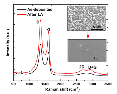
This successful wafer-scale integration was done through a pulsed laser deposition technique. The researchers used laser to confuse chemical groups and move electrons across groups, throughout the wafer. This effectively converted positively charged rGO to negatively charged rGO in a process of pulsed laser annealing using a nanosecond ArF excimer laser.
This wafer scale integration is done at regular room temperature and pressure and takes about 1/5th of a microsecond for completion. It results in a wafer with negatively charged rGO layered on the surface and positively charged rGO layered underneath.
The p-n intersection where the p-type and the n-type meet is extremely important for transistor applications. News of this scientific breakthrough has taken the world of researchers by storm as it has opened up a new frontier for further extensive research in Graphene-based functionalized 2D materials.