What is cache memory?
Cache memory is a high-speed memory. It is smaller than primary memory. But, it is faster than the Random Access Memory. The Central Processing unit can access it very quickly than the main memory DRAM. It is used to synchronize with the CPU for quick and better performance. It is significantly smaller but very faster memory. The Central Processing Unit can only access it. Cache memory refers to a particular hardware chip that helps the computer to create caches at various levels of the network. It is entirely different from the term cache. The cache memory is the fastest hardware in the memory hierarchy and almost the same speed as the processor.
It is costlier than the RAM but very economical than the CPU registers. It keeps the frequently requested data and instructions by the CPU. And deliver than immediately as and when requested by the CPU. In addition, it is a very fast memory; therefore, it acts as a buffer between the Main memory and the CPU. Besides, it is used to reduce the average time to access the data from the RAM. Further, it keeps the copies of the program data from frequently used from main memory locations so that the data is instantly available to the CPU as and when needed. Since it minimizes the time taken by the CPU to access data, it speeds up the site performance. And it may improve the memory latency.
Where is cache memory located?
The hardware that is employed as cache memory is High-Speed Static Random Access Memory (SRAM). It is placed within the CPU or in closer proximity to the CPU.
Cache memory is chip-based computer hardware. That store and retrieve the data from the primary memory more efficiently. It is a temporary storage area that the processor can retrieve the data more quickly. It is generally integrated with the CPU or placed on a chip that has a separate bus to connect directly. Because of its proximity to the processor, it is more quickly accessible and thereby increases the speed and efficiency of the system. Since it is significantly closer to the processing unit, it is smaller in size. And it is with lesser memory storage capacity than the RAM. Though it is smaller in size, it is a very complex chip. Therefore it is very expensive than the DRAM. It can respond to the request of the CPU in few nanoseconds, and therefore it is a hundred times faster than a DRAM.
What are the Levels of Cache Memory?
Traditionally it is categorized as levels. There are three general levels of it. The levels are based on their proximity and accessibility to the processor.
They are:
L1 Cache or Register –
L1 is the primary cache or first level of cache. It is very small but very exceptionally fast. Generally, it is embedded within the processor. The most commonly used register is accumulator, Program counter, address register, etc.
Here in L1, data is stored and accepted that are immediately stored in the CPU. If the processor is a quad-core CPU, then it will have 4 L1 caches. Since L1 is within the processor, it can work at the same speed as the processor. The L1 memory size is from 2KB to 64KB. The L1 cache further has two levels, namely Instruction cache and data cache.
The instruction cache stores the instructions required by the processor. And the data cache stores the data required by the processor.
L2 Cache or Cache Memory–
L2 is a secondary cache. Its memory storage is larger than L1.It may be embedded within the processor or be a separate SRAM chip. If it is external, then it is directly connected to the CPU by a high-speed system bus. Since it is connected by a separate bus, it cannot be slow down by the traffic of the main system bus. It is the fastest memory. It has a faster access time, and here the data is temporarily stored for quicker access.
All cores can have their own separate L2 cache, or they can share the one L2 cache among themselves. The memory size of each L2 is from 256KB to 512 KB. L2 is slower than the L1 cache. Intel introduced the very first L2 cache.
L3 Cache or Main Memory–
L3 is the main memory on which the computer works. It is small in size. It is located outside the CPU. And it is shared by all the cores of the CPU. Once the power is disconnected, the data will be erased. In addition, it is a specialized memory to improve the function of LI and L2. L1 and L2 are significantly faster than L3.
But L3 is double the speed of the DRAM. Each core will have dedicated LI and L2 in multicore processors, but they have common L3 to share. If L3 references as an instruction, then it is usually elevated to a higher level of cache. It is not present in all processors.Some high-end processors have this L3 cache. Its memory size is from 1MB to 8MB.
Technically speaking, modern CPUs have at least three independent caches. They are instruction cache, data cache, and translation looks aside buffer (TLB). The instruction cache speeds up the executable instructions and fetches the data.
The data cache speed up the data fetches and stores the data. The TLB is used to speed up the virtual to physical address translation for both executable instructions and data. However, the TLB Is not directly related to the CPU caches, and it is part of the memory management unit.
What are the types of memory Cache?
They are divided into two types Primary and Secondary.
The Primary Cache: The primary Cache (L1) is always located within the processor chip. It is smaller and very fast. The access time is almost similar to that of processor registers.
The Secondary Cache: The secondary cache functioning between the primary cache and the rest of the memory. It is usually of L2. Generally, this is also housed within the processor or in close proximity to the processor.
Purpose of Cache Memory:
The cache memory was introduced to reduce the speed gap between the processor performance and the memory performance to the minimum.
It keeps the data organized by relevance. And, it keeps the temporary files relevant to the system to complete the tasks required by the computer.
In addition, it unburdens the part of the information that is stored in the DRAM. So there will be no failure when it comes to the exchange of information due to over-saturation.
Advantages of Cache:
- It dissolves the data storage processes within the RAM
- Besides, it increases the processor response speed when executing and responding to the process’s request.
- It allows you to access newly viewed or uploaded files without consuming data.
- The reduction in the AAT
Disadvantages:
- If not correctly optimized causes problems with the processor and hinder the processor performance.
- If it fails, when deleting temporary files, it will overload itself with data and thereby slow down the data exchange process between the cache and the main memory and affect the system’s performance.
Why is Cache Faster than RAM?
Accessing RAM for each and every instruction may result in slow processing due to latency. We already know the clock speed depends on the time required to find and fetch the data from the RAM. In order to overcome the memory latency from the processor, a data cache is used. Whenever the processor requests data, it is fetched from the main memory and stored in the smaller memory called cache. If there is any further request for the same data, the cache is searched first. The structure resides closer to the processor both physically and in terms of the time taken to search and fetch data with respect to the main memory. That is why the cache is faster than RAM.
How Does Cache Memory Work with CPU Hand in Hand?
The first time, when the central processor needs the data, it looks inside the L1 cache for it. If it could not find it from L1, then it will check inside the L2 cache. And, if it finds the data, then the processor will process the data. If not, then it will move on to the L3 cache; if the data is not found in any of the cache levels, then it will look inside the RAM. Further, if the RAM also does not have the data, it will get the data from the system’s Hard Disk.
Therefore, when your computer system starts the first time, or an application or program is opened the first time, the data will not be available in the L1, L2, L3, or RAM. By that time, the processor unit directly gets the information from the hard drive. After that, when you open it again, the processor unit receives the data stored in the L1, L2, L3, or RAM.
How They Co-ordinate with Each Other:
The steps of the essential operation are here as follows:
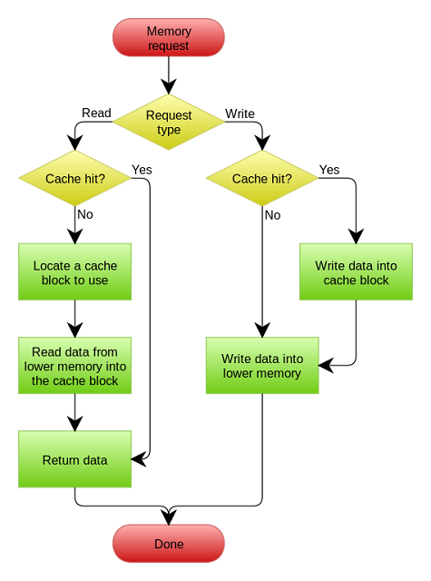
When the processor unit needs to access a particular data, the cache is checked for it. If it is found in the cache, it will read it from the L1, L2, or L3.
And if the data requested by the CPU could not be found in the cache, then the main memory is accessed to get the data.
Further, if not get the requested data from the RAM, then it will collect the DATA directly from the hard drive.
A copy of it will be stored in the main memory.
A block of data just accessed is then transferred from the main memory to the cache. The block size may vary from one to 16 characters.
The performance of the cache is measured in terms of the Hit Ratio.
When Central Processing Unit refers to the memory and finds the data in the cache, it is called Hit.
If the data is not found in the cache, then it is called Miss.
The ratio between the Hit and Miss plus Hit is called Hit Ratio. In other words, hit ratio is the ratio between numbers of hits by the total number of access (i.e., the total number of access= Hits+ Miss )
Cache Miss:
It is the number of failed attempts to read or write a piece of data in the cache. The cache miss results in the main memory access, which will take more time due to latency. There are three types of cache misses: instruction read Miss, data read Miss, and the data write Miss. The cache read Miss generally causes more delay because the processor needs to wait until the required data fetch from the RAM.
The cache read Miss from data cache usually causes less delay than the cache read Miss. Because the instructions are not dependent on the cache read, and the execution will continue until the data is returned from the primary memory for execution. Cache write misses to the data cache is the shortest delay. Since the write execution can be queued and there is very little limitation on the subsequent instructions. The processer can continue until the queue is full.
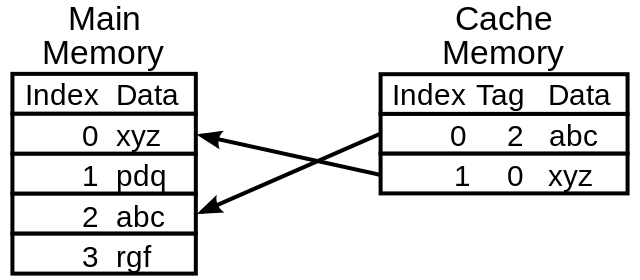
Cache Memory Mapping:
Cache Placement Policy:
The cache is a smaller memory that stores the recently utilized data by the CPU. The block of memory cannot be placed at random. It is stored in a single cache line or set of cache lines defined by the cache placement policy. Therefore the placement policy only determines where and when a particular memory block can be placed in the cache.
The memory mapping configuration continues to evolve. Earlier it was best described using the term Congruence Mapping. Now, there are three types of mapping policies available for the placement of a block in the cache. They are Direct mapping, Fully Associative Mapping, and Set Associative Mapping.
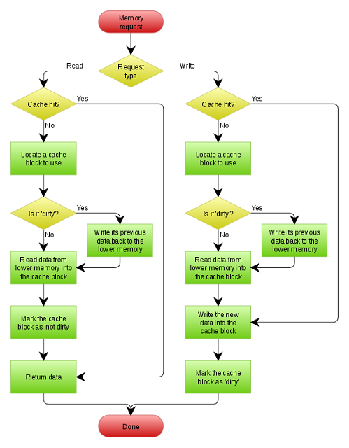
Cache Writing Policy:
When the system process writes the data to the cache, it follows some basic principles that are called writing policy. There are two types of policies they are write-through policy and write-back policy.
-
- In the write-through policy, writing is done synchronously both to the cache and the backing store.
- In the write-back policy, writing is only done on the cache very first. The writing to the backing store is postponed until the modified content is about to be replaced by another cache block.It is a very complex procedure to implement. It needs to keep the track record of which locations the data has been written over and mark them for later writing to the back store. The data at these dirty locations is written back by the backing store only when removed from the cache.
 Sometimes other policies may trigger data write back. Then it is explicitly notified to the cache to write back the requested data.
When no data is returned to the request on writing operation, a decision needs to be taken on the write misses, whether to write or not to write data into the cache. In this case, two policies are followed. They are Write allocate and No- write allocate.
Write Allocate (Fetch On Write)
In this case, data at the missed write locations are loaded to the cache following the write hit operation. In this case, the write misses are similar to read misses. The write-back cache uses write allocate for subsequent writes.
No-Write Allocate (Write-No-Allocate or Write Around)
In this case, data at the missed write location is not loaded to the cache and is written directly to the backing store. Therefore the data is loaded into the cache on read misses only. The write-through cache uses no-write allocate since subsequent writes have no advantage since they need to be written directly on the backing store.
The other entities may change the data in the backing store. Therefore the copy in the cache may be stale and obsolete. Similarly, when the client updates the data in the cache, copies of the data in other caches will be obsolete. In those cases, the communication protocol between the cache managers will keep the data consistent and updated using the coherency protocols.
Cache Replacement Policy:
Cache replacement algorithms or cache replacement policies that optimize instructions that hardware maintained structure can use to manage the cache of information stored on the system. It improves performance by keeping recent or often used data items in memory locations that are quicker to access. When the cache is full, this replacement policy chooses which item to discard or which item to be replaced to make room for the fresh ones. The hit rate and the latency are the primary factors that decide the replacement policy.
We already discussed hit ratio describes how often a search item is found in the cache. The latency of the cache is how long the cache takes to return the searched item. The most efficient and faster replacement strategies typically keep track of lesser-used information to reduce the time required for updating the information. The replacement policy is a compromise between the hit rate and the latency.
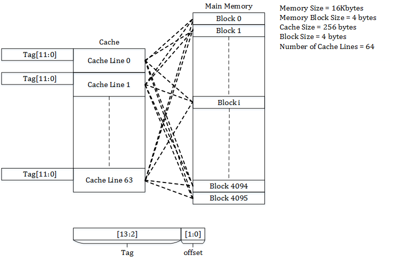
Direct Mapping:
Indirect Mapping structure, the cache is organized into multiple sets with a single cache line per set. Further, based on the address of the memory block, that can occupy a single cache line. The cache can be framed as n x 1 column matrix.
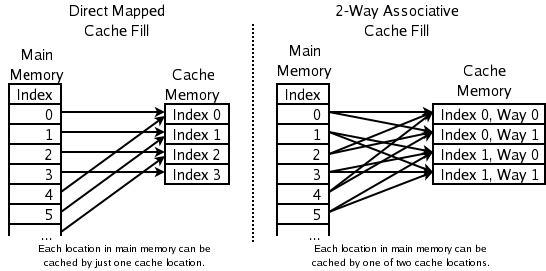
Each location in the main memory can go with only one entry in the cache. Therefore it is also termed as “one way set associative” cache. It does not have any placement policy. Thus there is no choice of which entry of cache contents is to evict. If two locations map is available to the same entry, then they may continuously knock each other out. Therefore it needs much larger space for better performance.
Let “p” be the block number in the cache.
“q” be the block number of the memory and further
“n” be number of blocks in the cache
Then mapping is done with the equation p=q (mod n)
How Block is Places in the Cache in Direct Mapping:
To place a block in the cache, the set is decided by the index bits derived from the memory block’s address. Memory blog is placed in the set identified, and related tag is stored in the tag field related to the set. If the cache line is already pre-occupied, then the new data replaces the memory block in the cache.
How the word is searched in Cache- Direct Mapping:
First, the set is identified by the index bits of the address
Next, the tag bits derived from them the memory block address compared with the tag bits associated with the set.
If both of the tag match, then there will be a catch hit. And the cache block is forwarded to the processor for processing.
If both of the tags do not match, then there will be a Catch Miss. And the right memory blog is fetched from the main memory or from the hard disk.
Pros and Cons of Direct Mapping:
Pros:
- Power-efficient
- Need not search through entire cache lines
- The placement and replacement policy is straightforward
Cons:
- Has lower cache hit rate (since only one cache line is available in a set)
- More conflict misses
Fully Associative Cache Mapping:
The placement policy only decides where a particular main memory entry must place in the cache. In Fully Associative Mapping, the placement policy is free to choose any entry in the cache to hold the copy of the primary memory data.
In Direct Mapping, each entry in the main memory goes in just one place in the cache. But many caches implement a compromise in which each entry in the main memory can go to any one of N places in the cache. So it is N-ways set-associative or full associative cache mapping. If more places to which the placement policy could have mapped a memory location, then it needs to check more places to check for cache entries. Therefore checking more places takes more power and chip area and more time.
At the same time with more associatively, it will have more cache hits and lesser misses so that it will save more time by minimizing time reading from the main memory. The latest CPUs can dynamically reduce the associativity of their caches in low power states to save energy.
How Block is Places in the Cache in Fully Associative Mapping:
The cache line is selected purely based on the valid bit associated with the entry. If the valid bit is zero, then the new memory block will be placed on the cache line. If not, it will be placed on another cache line with a valid bit zero. Further, if the cache is fully occupied, then a block will be evicted, and a memory block will be placed in that cache line.
The replacement policy will decide the eviction of the memory block.
How the word is searched in Fully Associative Mapping:
The memory address of the tag field is compared with the tag bits associated with all the cache lines. If It matches, then the block is present in the cache, and it is a cache hit. If it does not match, then it a cache misses. And it has to fetch from the lower memory. Based on offset, a byte is selected and returned to the processor.
Pros and Cons of Fully associative Cache:
Pros:
- Its structure provides the flexibility of placing memory blocks in any cache lines to utilize the cache fully.
- Because of the placement policy, it gets a better cache hit rate
- It offers more flexibility of utilizing a greater variety of replacement algorithms when a cache miss occurs
Cons:
- The placement policy is slow
- It takes more time to iterate all the lines
- It is power-hungry due to placement policy
- Most expensive due to the high cost of the associative comparison hardware.
Set Associative Cache Mapping: 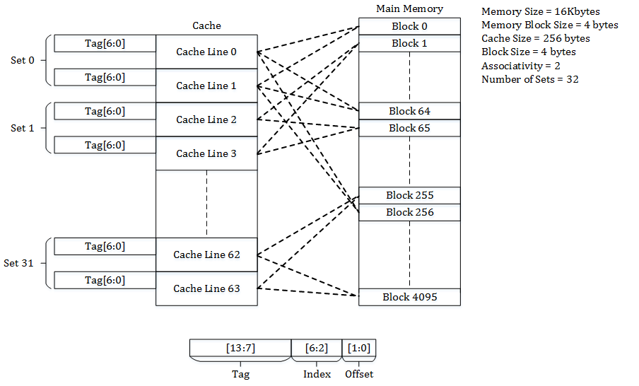
Set Associative Cache is the mean between the direct-mapped and fully associative cache. You may compare this cache to an m x n matrix. The cache is divided into n sets, and each set contains m cache lines. Any memory block is first mapped onto a set and then placed into any cache line of the set. The tags saved in the cache do not include the part of the main memory address. It takes less space on the processor since the cache tags have fewer bits that require fewer transistors.
Cache Hierarchy:
The latest processors have multiple interacting on-chip memory caches. Generally speaking, a particular cache can be specified by the size, bock size, a number of bocks in a set, cache write, and replacement policies.
Pipeline Cache:
These types of caches are specialized caches. They have at least three separate caches for instructions, TLB, and data. Each one works in a particular role. The design is to use a different physical cache for each. Pipelining technique tries to keeps all parts of the processor are busy engaging with some incoming instructions. The incoming instructions are divided into series of sequential steps performed by the processor units, with the instructions processed in parallel.
Victim Cache:
It is a cache used to hold blocks that are evicted upon replacement. It is at the middle of the primary cache and the refill path. Victim holds only those blocks of data that were evicted from the primary memory. It is used to reduce conflict misses. It was introduced in Haswell processors as an on the package.
Trace Cache:
Trace Cache is also known as execution trace cache. It increases the instruction fetch bandwidth and reduces the power consumption in Intel Pentium 4 microprocessors.
It stores the traces of instructions that are already fetched and decoded. Generally, trace cache stores instructions after it has been decoded or they were retired. When it is next time requested, it need not be decoded since it was already decoded and stored.
Write coalescing cache:
WCC is a special cache that is also a part of L2 in AMD microarchitecture. The purpose of write coalescing cache is to reduce the number of writes to the L2 cache.
Micro-operation (μop or uop) cache:
A Micro-operation cache is a specialized cache that stores the micro-operations of decoded instructions that were received from the instruction decoders or from the instruction cache When an instruction is needed to be decoded. The UC cache is first checked for the data to be reused. If it is not available, then the instruction is decoded and stored in μop or uop cache.
Fetching pre-decoded instruction eliminates the need for repeated decoding. And, it effectively offloads the fetch and decoding hardware, and therefore it minimizes the power consumption. μop or uop increases performance by delivering decoded micro-operations to the backend. Besides, it eliminates bottlenecks in fetch and decodes logic. It has better power efficiency; therefore, it is best suited for battery-operated devices.
Branch Target Instruction Cache:
The branch target cache is a specialized cache that holds the first few instructions at the destination of the token branch. It is generally used by low-powered processors, which do not need instructions. The memory system is fast enough to deliver instructions. It provides instructions for those few cycles avoiding delay after most taken branches when pipeline bubble happens. Branch target instruction cache allows full-speed function with a significantly smaller cache than the traditional full-time instruction cache.
Smart Cache:
It is an L2 or L3 caching method for multiple execution cores developed by Intel.In addition, it shares the entire cache memory between the cores of the multicore processors. Besides, it reduces the cache miss rate. Since all cores need equal allocation of cache space, a single core can use the entire L2 or L3.
Cache in Multicore Chips:
When discussing about the multicore chip, a question will arise whether the cache should be shared or local? If it is local, whether should it be implemented to each core? Etc. Introducing shared cache needs more wiring and complexity. But, having one cache per chip can reduce the space utilization so that one can introduce a larger cache into the limited space.
Sharing L1 will result in more latency and make each core run slower than the single-core chip. Having a global cache can allow a single core to use the whole cache to reduce data redundancy. For example, an eight-core chip with three-level may include an L1 cache for each core and L2 for each pair, and one L3 cache shared between all the cores. More techniques are employed to increase the parallelism when the Last Level Cache is shared between multiple cores, including slicing.
Hardware Caches:
CPU Cache:
CPU caches are the smaller memories that are on or very close to processors that can operate faster than the main memory. Modern computer systems have six types. They are entirely managed by hardware.
GPU Cache:
The older GPUs had limited read-only texture caches. Texture caches are read-only caches in the GPU for buffering map read.
It accelerated the texture sampling operation. The cache is vital for 32-bit or wider systems to transfers the texture data, which are in 4 bits per pixel, indexed in complex patterns. The advanced GPUs are having general caches, including instruction caches.
Cache Coloring or Page Coloring:
It is a process of allocating free pages that are neighboring from the processor cache point of view to maximize the total number of pages cached. The cache coloring is typically done by the low-level memory allocation code in the operating system when mapping virtual to the physical memory.
A virtual memory subsystem that lacks cache coloring is less deterministic with regards to cache performance, as differences in page allocation from one program run to the next can lead to large differences in program performance. The actual mapping from virtual color to physical color is not connected to system performance.
Software Caches:
Disk Cache:
There are varieties of software available to manage caches. The page cache in the main memory is an example of a disk cache. The system kernel manages the disk cache. Disk buffer is an embedded memory in the hard drive acting as a buffer between the system and the physical hard disk platter used for storage. The local hard disk drive can also cache information on the data storage devices.
Web Cache:
The web browsers and proxy servers use web caches to store the previous responses from the web servers. The web pages and images are stored in the web cache. It reduces the amount of data that needs to be sent across the network, and the browser reuses the previously stored data. This reduces the bandwidth usage and loading time of the web page.
It helps the responsiveness of the web page. The web browsers employ the built-in web cache. Some internet service providers also use caching proxy servers, which caches the page and shares it among those network users.
Another, peer-to-peer caching stores the p2p applications that are stored in the ISP cache to accelerate the peer-to-peer transfer.
Buffer Vs. Cache:
Buffer and cache are doing almost the same work. But the processing is different for both. In caching, the performance increase is due to the buffering that occurs within the caching system. You may realize that in the initial transfer of data. The read cache fetches data items from its residing location at least once. In order for subsequent reads of data, the data will be fetched from intermediate storage instead of the data residing location.
Similarly, with the write caches, the performance increase of writing data item, since it is stored in the intermediate storage after the first write. The caching process must adhere to coherency protocol to maintain consistency between the intermediate storage and the storage where the data is residing, and it is not in the case of buffering. Buffering reduces the number of transfers. It occurs for several small transfers over fewer larger transfers with the help of intermediary communication processes. It ensures the minimum data size required by at least one of the communication processes involved in the transfer.
With traditional caching implementations, a data item that is first read or written is successfully buffered. It increases the performance of the application.
Cache Vs. Buffer
Further, the portion of caching protocol where individual writes are deferred to batch writes is in the form of buffering. Similarly, the catching protocol where individual reads are deferred to a batch of reads also is a form of buffering. In general practice, caching almost involves buffering to some extent, and the strict buffering does not involve caching. Buffer storage is a temporary memory location that is used because CPU instructions cannot directly address data stored in peripheral devices. Therefore addressable memory is used as an intermediate.
Further, the buffer is a feasible solution when a large block of data is assembled or disassembled by a storage device. Besides, the entire buffer of data is usually transferred in sequence. The buffer itself sometimes increases transfer performance and reduces the variation of latency. The cache also increases the transfer performance. The sole purpose of it is to reduce access to the slower storage. Therefore the cache is also usually an abstraction layer that is designed to be invisible to the neighboring layers.